Zhao Zhigang, a researcher at the Suzhou Institute of Nanotechnology and Nano-Bionics, Chinese Academy of Sciences, and Zhang Dengsong, a professor at Shanghai University, conducted a detailed and in-depth study on this issue, and studied the nanocrystals of transition metal chalcogenides (WS2, MoS2, WSe2, MoSe2). Breakthrough progress has been made. The new method combines electrochemical and liquid phase stripping with Al3+ as the electrochemical insertion type ion and ethanol/oleic acid dispersion as the liquid phase stripping solvent. Under the discharge condition, the Al3+ large charge amount and high The impact property destroys the layered material, and further removes the Al3+ from the layer by using the good binding property of oleic acid and Al3+ in the liquid phase, thereby obtaining a single-layer nanocrystalline material having a uniform size and an average particle diameter of only 3 nm. The resulting WS2 nanocrystalline material can detect lower concentrations of trinitrophenol (TNP) with a detection limit of 10-6 M. The relevant research results are published in Chemical Communication (DOI: 10.1039/C6CC06325J).
Based on the above research results, Zhao Zhigang, a research group and researcher of Suzhou Nano Institute, and Zhang Fengxia, a professor at Suzhou University, cooperated to apply this stripping method to hexagonal boron nitride (h-BN) and cubic boron nitride (c-BN). Nanocrystals of two materials were also successfully prepared, and two boron nitrides were found to have significant differences in piezoelectric properties. Compared with the corresponding bulk materials, the piezoelectric properties of the stripped nanocrystalline materials are significantly improved, wherein the cubic boron nitride nanocrystals have a piezoelectric coefficient of 25.7 pC/N, while the cubic boron nitride blocks The piezoelectric coefficient of the body is only 4.3 pC/N, and the piezoelectric property of the nanocrystalline material is six times higher than that of the bulk material. Even if it is a boron nitride nanocrystal, the cubic structure is superior to the hexagonal piezoelectric property. The main reason is that the crystal structure of cubic boron nitride has a more obvious external force response. This study provides a new idea for promoting the development and application of cubic boron nitride as a superhard material. This research was finally published in Nano Letters (DOI: 10.1021/acs.nanolett.6b04272).
This series of work has received strong support from the National Natural Science Foundation of China and the Jiangsu Outstanding Youth Fund.
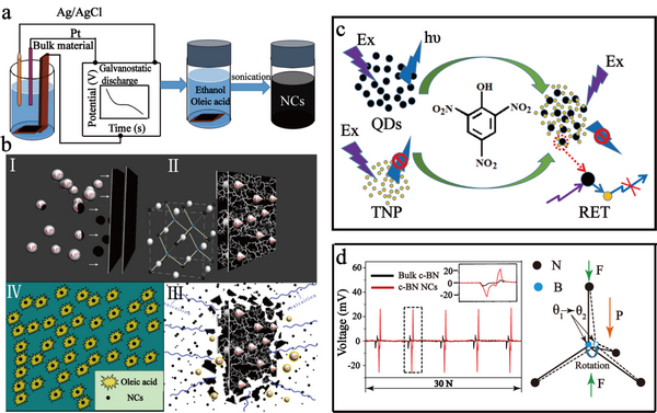
(c) Schematic diagram of trinitrophenol for detecting tungsten sulfide nanocrystals; (d) Schematic diagram of piezoelectric output and piezoelectric generation of cubic boron nitride nanocrystals
Spray Grain Texture Pu Sandwich Panels
Rich selection of textures and colors meet different decoration requirements, giving the city and the buildings a new look.
The PU foam is the most advanced and eco-friendly insulation material in the world. With the help of the back aluminum foil, the thermal preservation effect achieves the best.
The unique structure prevents the heat loss in winter. Meanwhile it reduces the heat of the summer sunshine.
Aceta paintcoat and flurocarbon paint of weather resistance performance are applied on surface of wall panel. It is reserved with superior self-cleaning, weather resistance, corrosion resistance and acid& alkali resistance performance.
Light weight with 3.7Kgs/m2 makes the installation easy.
The installation process is clean and tidy without any noise and dust, construction waste.
Different selections of accessories meet different effects.
High quality and stable performance: Manufactured in CNC automation production line, the product pass rate can reach 99.9% with stable chemical structure and physical structure.
Spray Grain Texture PU Sandwich Panels
Metal Cladding Panels,Insulation Metal Cladding Panels,Spray Grain Texture Pu Sandwich Panels,Spray Grain Texture Pu Sandwich Panels
Jinan Zhengtang Insulation Decoration Material Co.Ltd , https://www.ztwallsiding.com